FuriosaAI RNGD#
RNGD is FuriosaAI’s second-generation Neural Processing Unit (NPU) designed to accelerate deep learning inference. The NPU natively supports a broad spectrum of workloads, including high-performance Large Language Models (LLMs), multi-modal models, and vision-based neural networks.
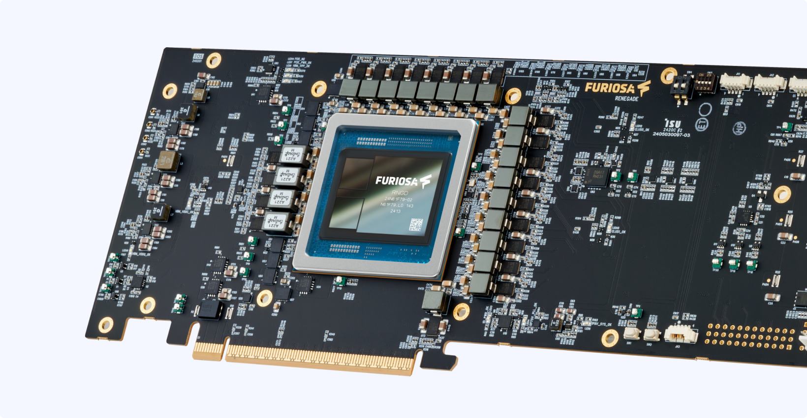
RNGD implements the Tensor Contraction Processor (TCP), a novel architecture designed to natively execute complex tensor contractions—the core mathematical operations underlying modern deep learning—directly in hardware. By leveraging this paradigm, the NPU maximizes both compute utilization and energy efficiency. Fabricated on TSMC’s 5nm process node and operating at a 1.0 GHz clock frequency, RNGD delivers high-throughput execution across diverse precision formats, achieving 256 TFLOPS for BF16, 512 TFLOPS for FP8, 512 TOPS for INT8, and 1024 TOPS for INT4 workloads. To sustain these compute throughputs without memory bottlenecks, the chip integrates two HBM3 modules that provide an aggregate memory bandwidth of 1.5 TB/s. Furthermore, it interfaces with the host via PCIe Gen5 x16, ensuring low-latency data movement.
In addition to its core compute capabilities, RNGD seamlessly integrates into cloud-native and multi-tenant environments like Kubernetes. By implementing Single Root I/O Virtualization (SR-IOV), the system allows a single physical chip to be partitioned into 2, 4, or 8 independent NPU instances. Each virtual instance operates with strict hardware isolation, utilizing its own dedicated compute cores and private memory bandwidth to guarantee deterministic latency for co-located workloads.
For a detailed technical analysis of the TCP architecture and the RNGD implementation, please refer to the following publications:
TCP: A Tensor Contraction Processor for AI Workloads (ISCA 2024) (PDF)
FuriosaAI RNGD: A Tensor Contraction Processor for Sustainable AI Computing (Hotchips 2024)
Tensor Contraction Processor: The First Future-Proof AI Chip Architecture
Architecture |
Tensor Contraction Processor |
Process Node |
TSMC 5nm |
Frequency |
1.0 GHz |
BF16 |
256 TFLOPS |
FP8 |
512 TFLOPS |
INT8 |
512 TOPS |
INT4 |
1024 TOPS |
Memory Bandwidth |
HBM3 1.5TB/s |
Memory Capacity |
HBM3 48GB |
On-Chip SRAM |
256MB |
Interconnect Interface |
PCIe Gen5 x16 |
Thermal Solution |
Passive |
Thermal Design Power (TDP) |
150W |
Power Connector |
12VHPWR |
Form Factor |
PCIe dual-slot full-height 3/4 Length |
Multi-Instance Support |
8 |
Virtualization Support |
Yes |
SR-IOV |
8 Virtual Functions |
ECC Memory Support |
Yes |
Secure Boot with Root of Trust |
Yes |